
AS3310 Voltage Controlled ADSR
Published Mar 2025 · 1 min read
This module is licensed under the MIT License
TODO
- Schematic
- Build prototype
- PCB Design
Introduction
This module is a simple VC ADSR design. The design is based on the chip’s datasheet info.
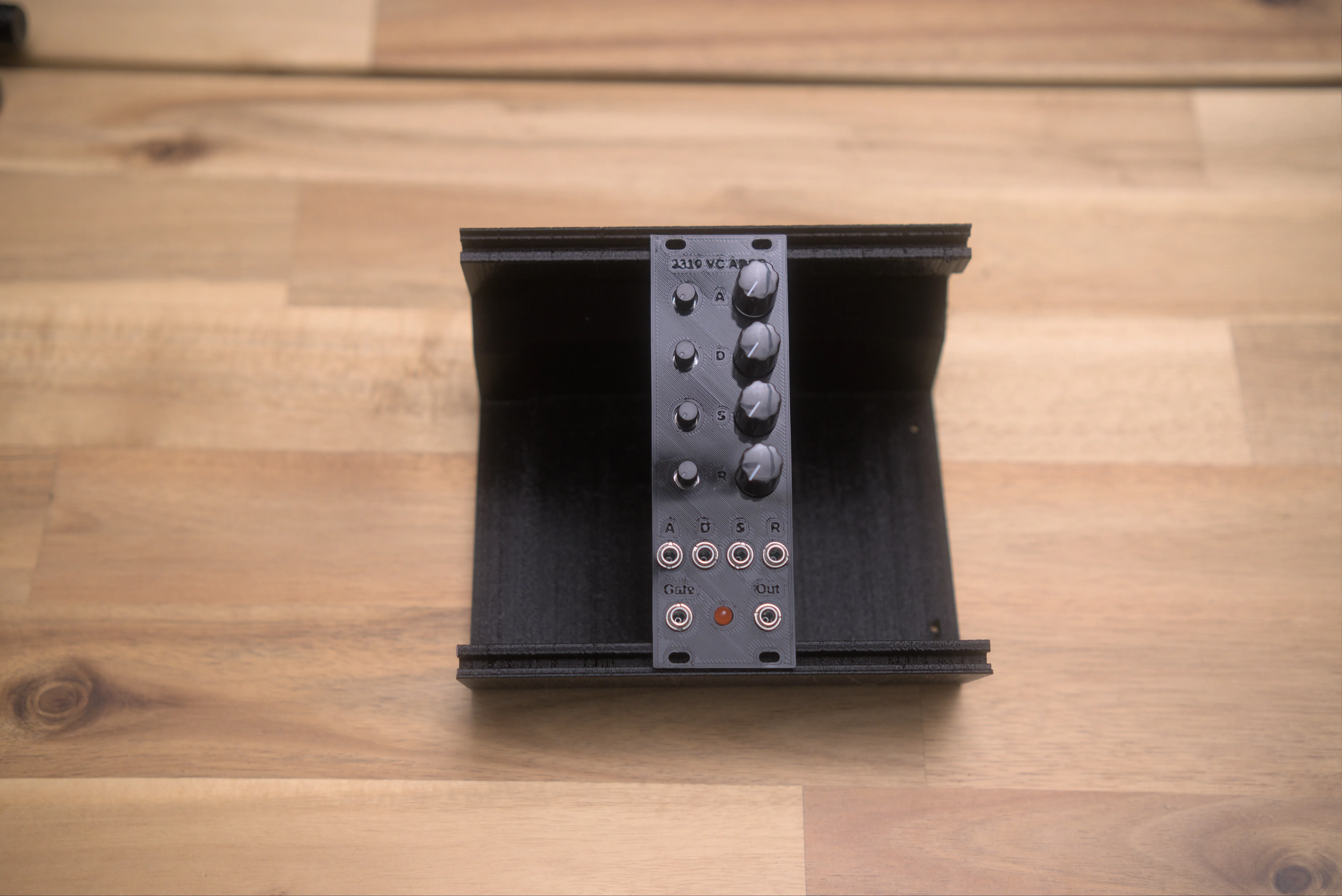
Module Images
Demo
Module Features
Each envelope parameter is CV controllable (Attack, Decay, Sustain, Release)
I/O and Controls
Inputs:
- Gate input (0-5v, 0-10v)
- Attack CV input (10vpp)
- Decay CV input (10vpp)
- Sustain CV input (10vpp)
- Release CV input (10vpp)
Output:
- Envelope output (0-5v)
Controls (knobs):
-
Attack input attenuation knob
-
Attack offset knob (serves as control knob when no input is connected)
-
Decay input attenuation knob
-
Decay offset knob (serves as control knob when no input is connected)
-
Sustain input attenuation knob
-
Sustain offset knob (serves as control knob when no input is connected)
-
Release input attenuation knob
-
Release offset knob (serves as control knob when no input is connected)
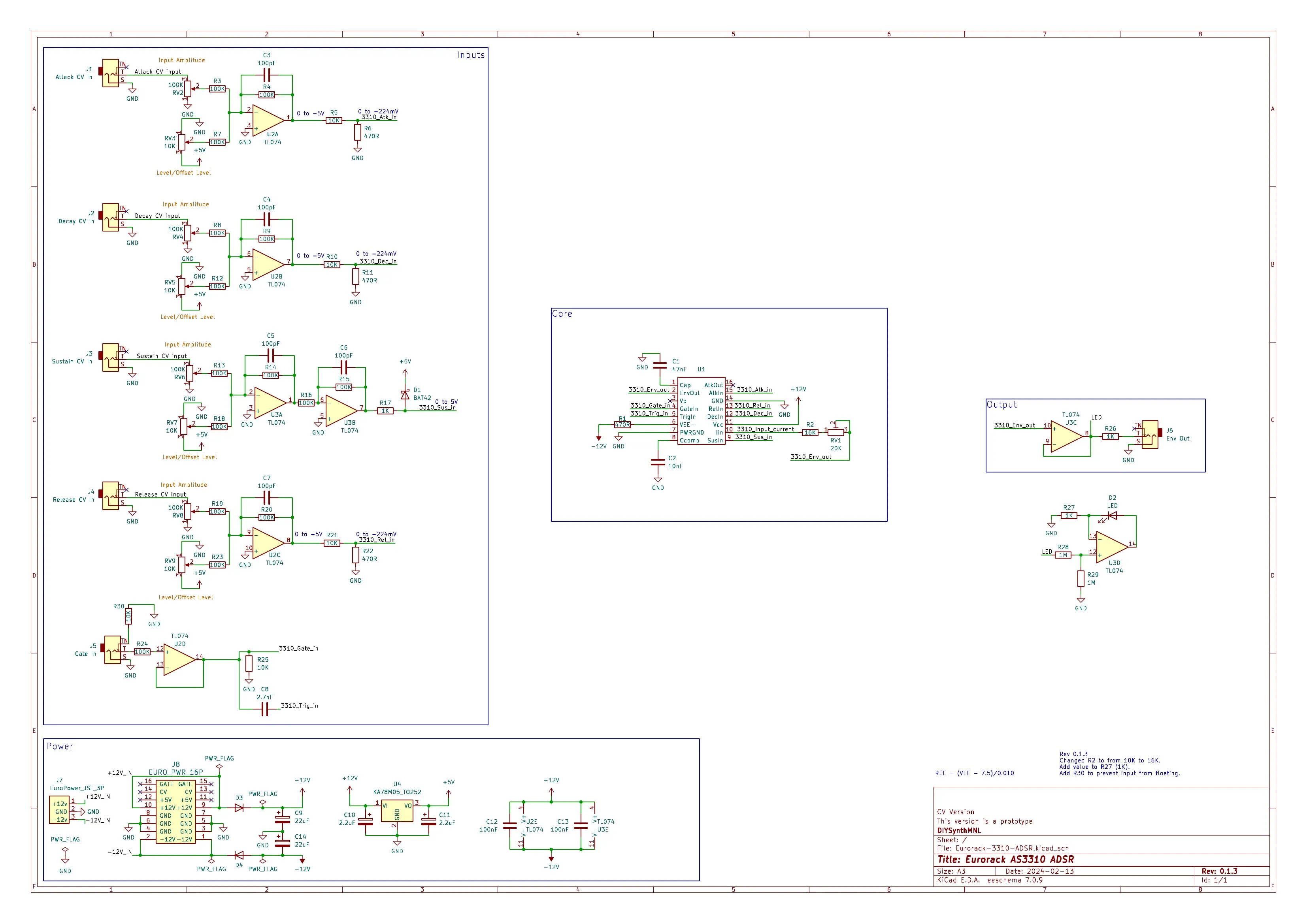
Design Notes
The Attack, Decay, and Release CV inputs are inverting mixers.
The sustain circuit is a combination of an inverting mixer and an inverting amp with a gain of 1 to invert it back in phase. A schottky diode clamps the positive voltage to +5v.
Check out the falstad circuit simulation here
Schematic
Conclusion
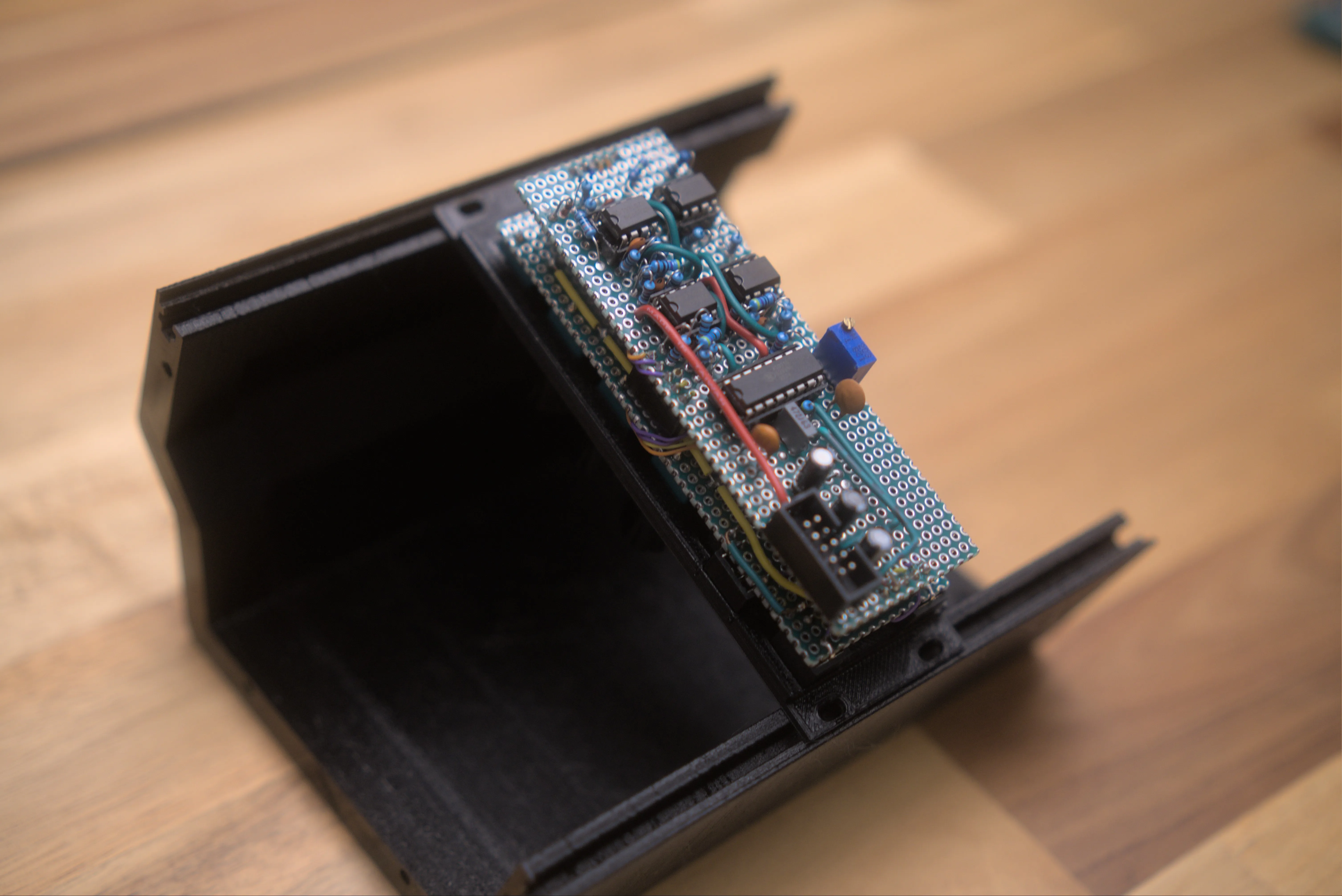
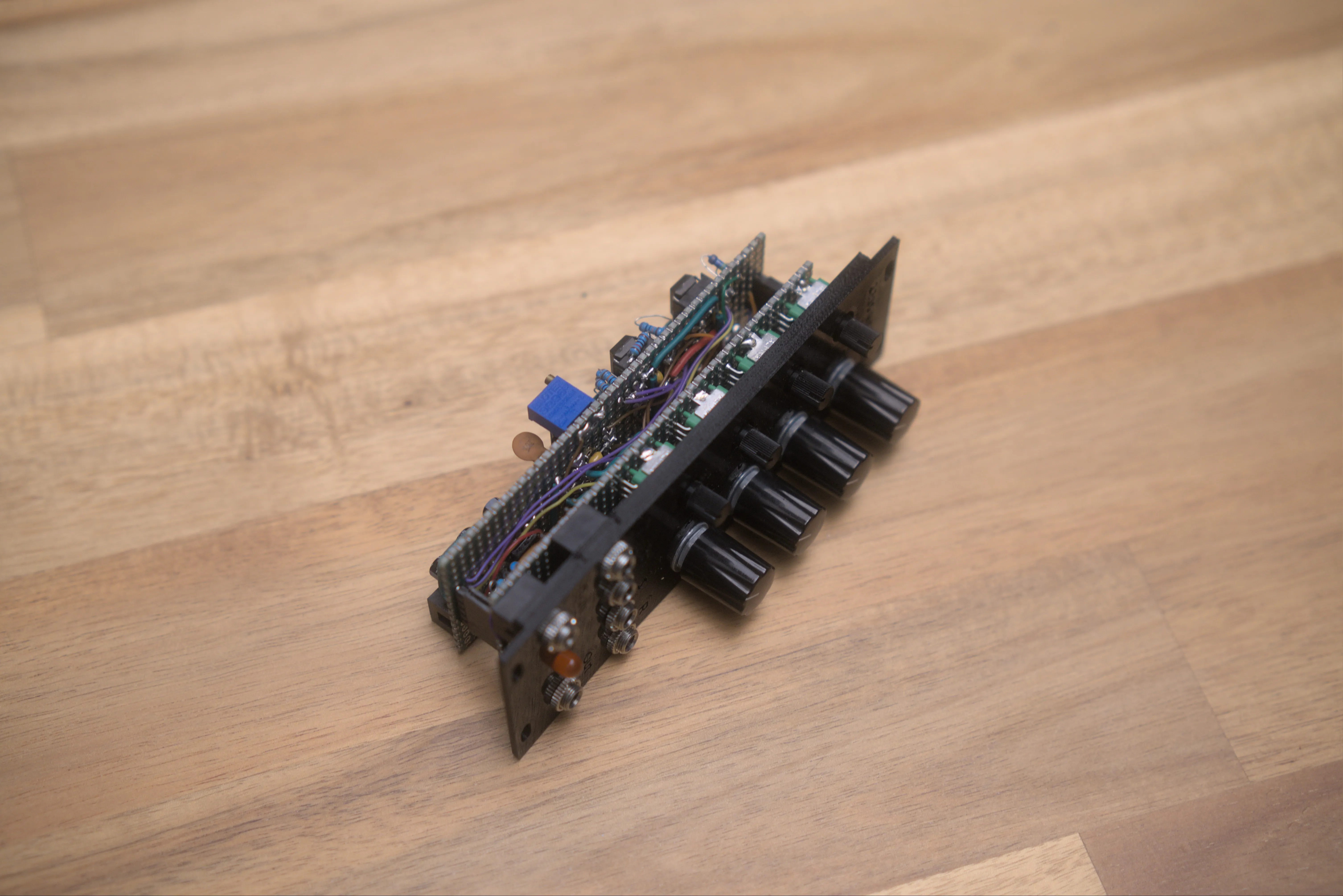
If you’d like to build this module, I have provided a 3D printed front panel file in the repo. I used readily available green perfboard. The components should line up with the perfboard’s holes. The panel was made using benjiaomodular’s europanelmaker.